Circuit Design and Prototyping
When researching different approaches to essentially create two timers, one for the heart and one for the pacemaker, the astable (or free-running) multivibrator caught my eye. I could have used, say, a quartz crystal oscillator, but I felt like this wasn’t “natural,” in the sense that how such a component worked wasn’t immediately intuitive to me, and probably wouldn’t be to others.
But an astable multivibrator can be explained in a relatively simple manner: there are two “buckets” of charge, or capacitors, and only one can be filled at a time. Each bucket takes the same amount of time to fill every time, so when a bucket is filled, it can be emptied into a pipe at a regular interval. Furthermore, every component in an astable multivibrator circuit, and especially the capacitors, can easily be seen on a circuit board.
Astable Multivibrator
But what exactly is an astable multivibrator? According to this source, it is a free-running, oscillating circuit that continuously switches between two states, thereby producing two square wave output waveforms. In other words, it’s a circuit that creates two pulses at a regular interval.
An aside
The astable multivibrator was especially fascinating to me because I had just learned about latches, or cross-coupled transistors, in my digital design class.
According to the linked source above, cross-coupled transistors are the core of each of the different types of multivibrators, like monostable, bistable, and astable.
In fact, latches are a type of bistable multivibrator, since they have two stable (or resting) states: high or low. The "astable" in "astable multivibrator," therefore, means that the circuit does not have a stable or resting state. This makes sense when considering the fact that the circuit is relentlessly switching between high and low at its two outputs.
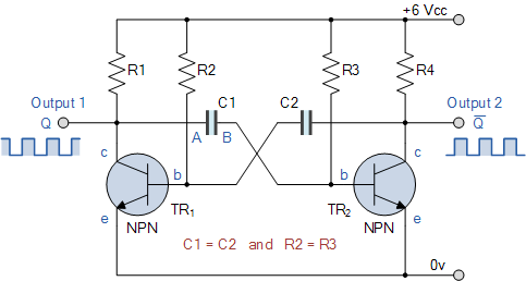
And how does it work? Looking at the circuit above: say TR1 is off and TR2 is on. Then Plate A of C1 is essentially connected straight to Vcc (6V) as there is no voltage drop through R1 (no current is flowing through the resistor since TR1 is not conducting any).
Plate B of C1 has about 0.6V because standard NPN transistors usually require a base-emitted voltage of 0.6 to 0.7V. This creates a potential difference of 5.4V across C1.
Since TR2 is on, C2 starts to charge up, and as soon as it reaches this 0.6V threshold, it turns TR1 on, causing Plate A of C1 to fall to 0V (with ideal components). This happens because TR1 acts like a closed switch that connects Plate A of C1 straight to ground.
The drop in voltage from 6V to 0V on Plate A of C1 causes an equal and instantaneous drop in voltage on Plate B, pulling it down to -5.4V. This reverse voltage turns TR2 off.
Since TR1 is now on and TR2 is now off, C1 begins to charge up from -5.4V towards the 6V supply. As C1 reaches 0.6V, though, it turns TR2 back on and TR1 off. Now, the circuit is back to the state described originally, and the whole process repeats again, and again, and again.
Heartbeat Circuit
I decided to design and prototype the hearbeat circuit first. This circuit would blink an LED on and off at a standard resting heart rate (60 to 100 beats per minute).
Circuit Schematic
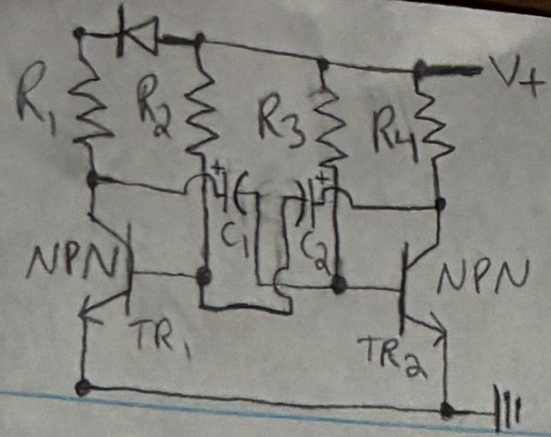
I began by recreating the astable multivibrator circuit diagram shown above. However, I made a small mistake: to try to simplify the circuit, I put the LED in series with R1 instead of in parallel with TR1. I did not realize what effect this would have on the circuit until much later…
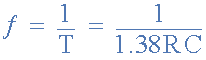
To determine the effect on the circuit timing that values for R2, R3, C1, and C2 had, I used the time constant formula depicted below. This formula is derived from the standard capacitor voltage vs. time equation. The resistors R1 and R4 do not affect the timing significantly if they are much smaller then R3 and R4, and they primarily limit the current going through the output, meaning that for an LED, they should usually be between 100 and 1000 ohms.
The biggest capacitor I initially had access to was 22 microfarads, so I started with that for C1 and C2. I then picked a large resistor, 1 megaohm, for R2 and R3 to slow the pulsing of the LED down to a low frequency so that I could easily measure the period. This would allow me to compare the theoretical period of about 30 seconds with the actual period and ensure that my circuit was built correctly.
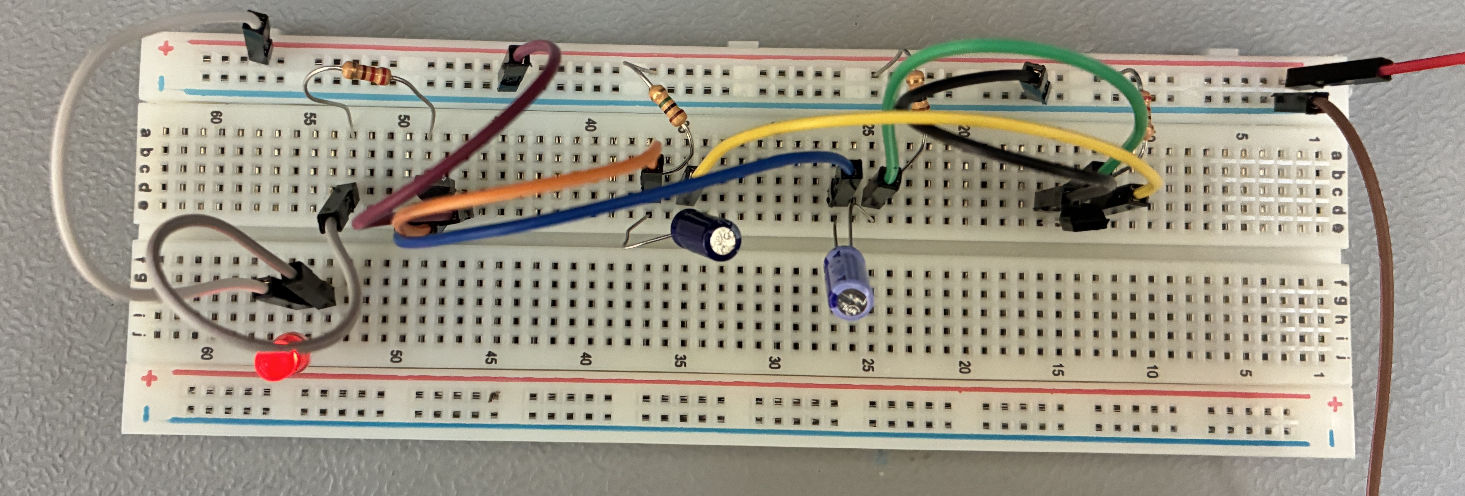
Prototyping
I used a breadboard to prototype this circuit, and I used an Arduino Nano’s 5V and GND pins to provide 5V power. When I put this circuit together on the breadboard, the measured period was way off from the theoretical period. The LED was blinking every 2-3 seconds instead of once every 30 seconds.
Problem
The LED was blinking 10 times faster than it should’ve been!
I tried 100K ohms for R2 and R3 instead of 1 megaohm, and I also procured 10 microfarad capacitors. This should have decreased the period down to about 1.38 seconds. To measure the tiny period, I used an online beats-per-minute counter that musicians use to keep time. I tapped the button each time the LED turned on, and I was then able to find a period of about 0.75 seconds. This was still way off!
To understand why my circuit timing was off, I searched the web for more tutorials, forums, and troubleshooting tips. Ultimately, I found two things that seemed to be causing the problem:
- Asymmetry: Usually, components are connected to each of an astable multivibrator’s two outputs, as shown in the schematic above. I connected an LED to just one output (“Output 1”) and did not use the second output. Here’s why this is a problem:
- While the LED is off, TR2 is on. Because TR2 has no LED connected to its collector, it functions as expected:
- While Q2 is OFF, its collector charges all the way up to 5V.
- When Q2 turns ON, its collector drops to 0V (ideally). This is a voltage swing of 5V.
- This drop pushes the base of Q1 down from 0.6V by 5V. Thus, C2 starts at -4.4V.
- Using the universal RC charging formula, Vt = Vf + (Vi - Vf)*e^(-t/RC), we solve for t by plugging in 5V for Vf, 0.6V for Vt, and -4.4V for Vi. This gives t = 0.76 seconds.
- While the LED is on, though, TR1 is on. Because the LED drops about 2V, TR1 does not behave normally:
- While Q1 is OFF, its collector charges only up to 3V because of the LED’s voltage drop.
- When Q1 turns ON, its collector drops to 0V (ideally). This is a voltage swing of 3V.
- This drop pushes the base of Q1 down from 0.6V by 3V. Thus, C2 starts at -2.4V.
- Using the universal RC charging formula, we solve for t by plugging in 5V for Vf, 0.6V for Vt, and -2.4V for Vi. This gives t = 0.52 seconds.
So, the LED is off for longer than it is on, and the total period should be about 1.28 seconds, not 1.38 seconds. This changed the formula for the period to T = 1.28*R*C. However, 1.28s was still very far from the measured period, which brought me to the second culprit.
- While the LED is off, TR2 is on. Because TR2 has no LED connected to its collector, it functions as expected:
- Base Starvation: Using 100K ohm resistors for R2 and R3 restricted the base current for each transistor to just 44 microamps (4.4V/100K), meaning that transistors were not fully opening. Thus, their collectors were not dropping down to 0V, but instead to a slightly higher voltage, shrinking the voltage swings and thus the period.
- The 2N2222 transistors I used typically have a gain of about 100, meaning 1 microamp of current into the base allows 100 microamps to flow through the collector. However, this ratio may not always allow the transistor to turn fully on. Using Forced Beta, or assuming a gain of only 10, ensures that the transistor turns on completely.
- Since I used 220 ohm resistors for R1 and R4, the LED was able to draw up to 23 milliamps, meaning that a base current of 2.3 millamps was required to allow this current through the transistor (assuming Forced Beta). Thus, the 44 microamps present at the base was much too low.
To eliminate the base starvation, I made three changes:
- First, I increased R1 and R4 to 1K ohm resistors. This made it so that the LED could only draw up to 5 milliamps, which is still enough to light up properly. This reduced the amount of current the base needed to about 500 microamps.
- Second, I decreased R2 and R3 to 6K ohms. This increased the current available at the base to about 730 microamps (4.4V/6K), well above the 500 microamps needed.
- Third, I changed C1 and C2 to 100 microfarad capacitors. I did this to cancel out the change in timing caused by decreasing R2 and R3. Decreasing the resistance by a factor of about 20 required me to increase the capacitance by about a factor of 20, and the largest capacitor I could get was 100 microfarads, which were a factor-of-10 increase from the 10 microfarad capacitors. Thus, I expected my period to be reduced by about a factor of 2. Accounting for asymmetry and base starvation, the theoretical period was T = 1.28*6K*0.0001 = 0.768 seconds, which checked out with my estimate of 1.28/2 = 0.64 seconds.
Using the online BPM counter again, I measured the actual period to be about 0.71 seconds. This was much closer to my calculated estimate of 0.768 seconds, and accounting for component tolerances (20% for the capacitors) meant that the two periods matched very well. Moreover, I now had a LED that blinked every 0.71 seconds, or at about 85 BPM, perfect for mimicking a standard resting heart rate.
Pacemaker Circuit
I then recreated the heartbeat circuit and modified the components to blink the LED at a slightly slower rate. Most demand pacemakers begin pacing at about 60 BPM, so my goal was to blink the LED at this rate.
I changed R3 and R4 from 6K to 7.1K. This increased the theoretical period to about 0.91 seconds, leading to an expected rate of 66 BPM.
I measured the actual period to be about 0.83 seconds, giving an actual rate of about 72 BPM. This was visibly below the 85 BPM of the heart and not too far from 60 BPM, so I was satisified.
Combined Circuit
Next, I needed to combine the heartbeat and pacemaker circuits into a single circuit. This circuit would have to blink the LED on and off at the heartbeat rate of 85 BPM. It would have to have a wire that could be disconnected to stop the heart, and a method for the pacemaker to sense the stopped heart and take over for the heart at about 72 BPM.
Thus, there were two main challenges I had to solve:
- Determine how to keep the pacemaker off until it sensed that the heart stopped “beating” (someone unplugged the wire), and then turn the pacemaker on.
- Figure out how to merge the separate heartbeat and pacemaker outputs into a single LED.
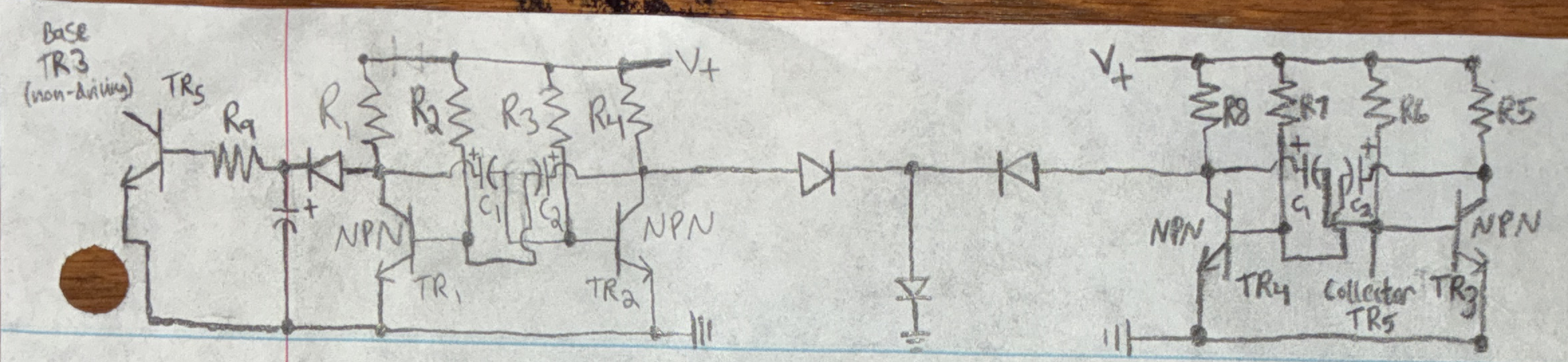
Sensing
To solve the first challenge of sensing a stopped or irregular heartbeat, my initial approach was as follows:
- In the pacemaker circuit, I connected the collector of a new transistor to one leg of C2 and the emitter to the other leg of C2.
- I then connected the base to “Output 1” of the heartbeat circuit.
My goal with this approach was to short the capacitor and empty its stored charge every time the heart output turned on by using the heart output to switch on the new transistor that I connected across the capacitor. However, this didn’t work, probably because there was no path to ground for the capacitor to discharge into. The pacemaker circuit kept on blinking its LED.
Also, I realized that this approach was flawed because the heart could still be blinking properly even if the output was off, since there would be a period of time when it had to be off every cycle. Thus, if the two cycles were offset in a certain manner, C2 of the pacemaker could still charge up and eventually turn on “Output 1” of the pacemaker.
While reviewing my circuit schematic to come up with a new approach, I noticed a new problem. I had placed the LED in each circuit in series with R1 instead of placing it in parallel with TR1. This meant that every time TR1 switched on, the LED switched on.
In a standard astable multivibrator circuit, though, every time TR1 switches on, the output switches off, and vice versa. This happens because, when TR1 switches on, the current coming out of R1 has a direct path to ground, which it would prefer to take instead of going through the LED, which forces the LED off. When TR1 switches off, the only path the current has to ground is through the LED, thereby turning the LED on.
My subsequent approach was to use the output of the heartbeat circuit to charge a capacitor. This capacitor would charge during the time the output of the heartbeat circuit was on, and would then discharge during the time the output was off. It would discharge into the base of a new transistor.
The collector of this transistor would be connected to ground to create a path from the emitter to ground. And instead of connecting the emitter to C2 of the pacemaker circuit, I would connect it to the base of TR2 of the pacemaker circuit, thereby pulling the base to ground and turning TR2 off every time the heart turned on. This would force TR1 to be on because of the opposite nature of TR1 and TR2, thereby turning off the output of the pacemaker circuit.
If the hearbeat circuit turned off and missed a cycle, the capacitor would not charge up and then discharge in time to turn TR2 off before C1 naturally turned TR2 on, thereby turning TR1 off, turning the output of the pacemaker circuit on, and finally allowing the pacemaker to take over.
This approach also solved the potential problem that the first approach had: incorrectly assuming the heartbeat was stopped while the heart output was off.
Merging
To solve the second challenge of merging the separate circuit outputs into a single LED, I decided to connect standard 1N4007 diodes to the output of each circuit. The anode of each diode connected to the output, and the cathode connected to the LED. Because of the diodes, the output current from the heartbeat can flow into the LED, and the output current from the Pacemaker can flow into the LED, but they cannot flow backward into each other.
Final Circuit
Below is the final circuit schematic.
Watch me demo the circuit by clicking the link on the left sidebar.